Capital Region Ushers in the Post-Scaling Era with Chip Stacking R&D
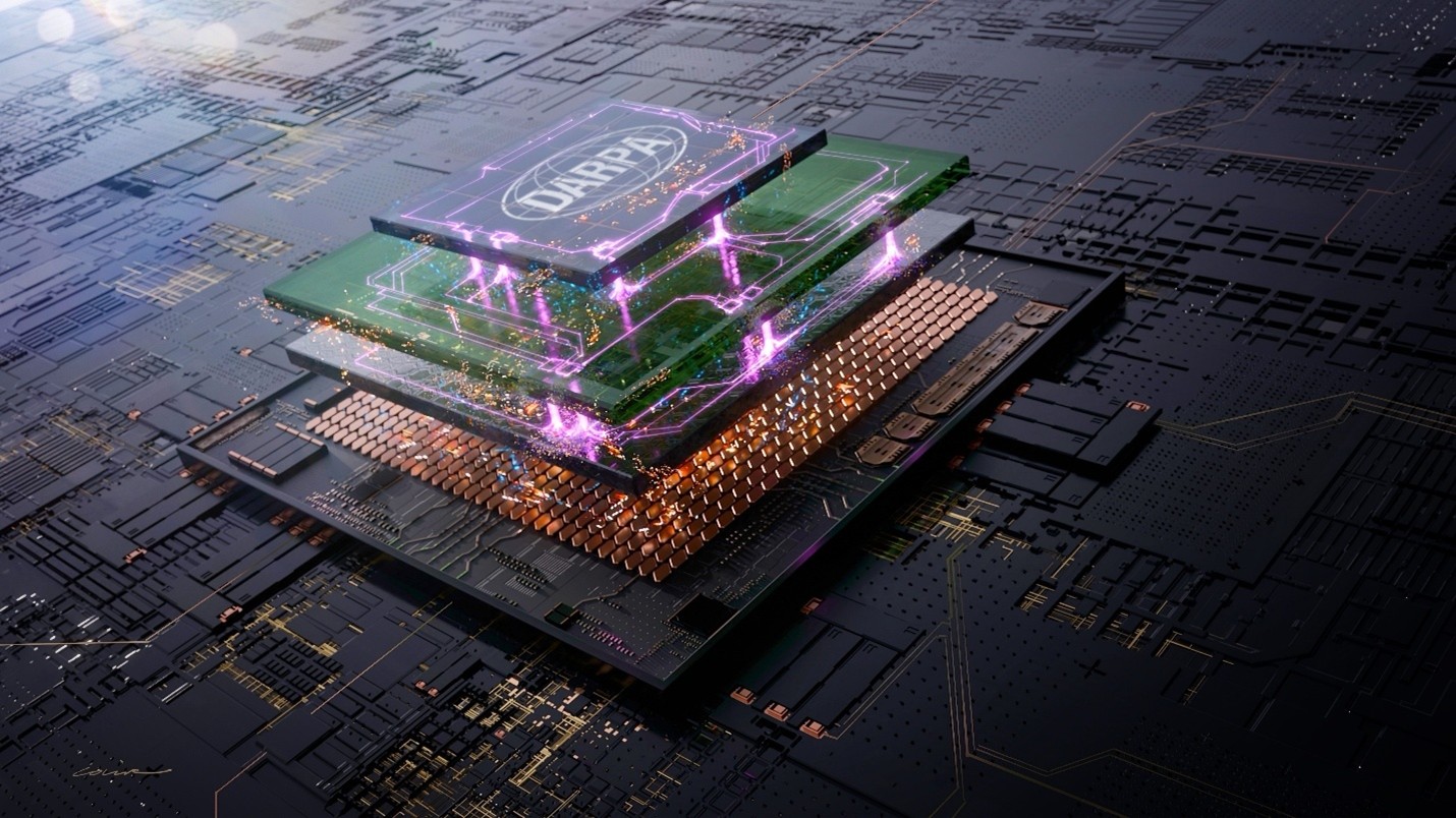
Notional rendering of 3D heterogeneous integration (3DHI). Courtesy of DARPA.
Highlights:
- NY Creates and partners at its Albany NanoTech Complex pioneer 3D heterogeneous integration (3DHI) R&D as the semiconductor industry enters the post-scaling era.
- IBM Research, GlobalFoundries, GE Aerospace are involved in DARPA projects related to 2.5D/3DHI R&D.
- Local semiconductor startups get DARPA funding for 2.5D/3DHI-related R&D.
- Albany-based researchers from IBM Research, Applied Materials, Tokyo Electron, and AIM Photonics publish papers highlighting 2.5D/3DHI innovations.
- IBM Research expands collaboration with TEL, ASMPT and Rapidus for R&D on 3D stacking and/or chiplet technologies.
The Capital Region is playing a leading role in taking the semiconductor industry in a new direction: vertically, as the focus of R&D shifts from shrinking chips through traditional 2D scaling to the vertical stacking of diverse chiplets to create compact, ultra-high-performance packages via a process called 3D heterogeneous integration (3DHI).
Later this year, the High NA EUV Lithography Center at NY Creates’ Albany NanoTech Complex will start providing high NA EUV lithography, in addition to its existing standard NA EUV lithography capabilities. The introduction of high NA EUV lithography will enable the development of the most advanced chips that then can be assembled into a 3D package. The new facility, when combined with GlobalFoundries’ planned advanced packaging center in Saratoga County, positions the Capital Region to become a major 3DHI R&D hub.
“NY Creates facilitates the fabrication of powerful semiconductor chips with our industry partners, as well as the 3D heterogeneous integration of memory, logic, and photonics at our Albany NanoTech Complex,” said Dave Anderson, President of NY Creates. “We offer accessible standard EUV lithography—and soon High NA EUV lithography—to make those chips that are then processed and assembled into a 3D package. Our High NA EUV Lithography Center will raise the bar for New York’s Capital Region, New York State, and the U.S. by anchoring the world’s most advanced lithography resources in one cooperative ecosystem. In collaboration with industry and academic partners, these efforts are strengthening the region’s semiconductor R&D leadership, driving workforce development, and bolstering economic growth efforts.”
For more than two decades, researchers have been anticipating the “post-scaling era,” a term that was coined by IBM in 2002. By leveraging EUV lithography tools at Creates’ Albany NanoTech Complex, IBM Research has pushed the boundaries of 2D scaling through innovations such as its 2 nm chip technology. Even as Albany NanoTech Complex researchers prepare for R&D on sub-2 nm nodes, the emphasis is not only on further shrinking chips but also on stacking chiplets that integrate logic, memory, compute, and other functions.
Importantly, both the White House and federal Departments of Commerce and War are prioritizing R&D for 3DHI, which is seen as “a key driver of next-wave electronics performance.” The post-scaling era is already here, in New York’s Capital Region. Below are examples of the 2.5/3DHI R&D underway in the region.

In January 2025, GlobalFoundries announced plans to build a $575 million New York Advanced Packaging and Photonics Center in Saratoga County. This first-of-its-kind center will support the assembly and testing of 3D and heterogeneous integration chips using GF’s 2nm FinFET (12LP+) and 22nm fully-depleted silicon-on-insulator (22FDX), among other platforms. The center will focus on the advanced packaging and testing of chips for artificial intelligence (AI), automotive, aerospace and defense applications.
In addition to the $575 million packaging center, GF pledged $186 million for R&D over 10 years. Six months later, last June, GF pledged an additional $3 billion for expansions and upgrades to its New York and Vermont fabs, bringing its total investment to $16 billion. GF stated the additional investment will include R&D for initiatives focused on packaging innovation and silicon photonics, which are centered in Malta.
Eighteen months before GF announced plans for the New York Advanced Packaging and Photonics Center, it forged a strategic partnership with Lockheed Martin for the secure manufacturing of next-generation chips, including “3D heterogeneous integration for optimized chip packaging that improves performance.” GF and Lockheed Martin also pledged to “work to develop a chiplet ecosystem to produce chips more rapidly and affordably.”
GF’s Fab 8 in Malta is a Department of War trusted foundry that is authorized to manufacture chips for national security systems. When announcing the advanced packaging center, GF President and CEO Thomas Caulfield emphasized that the facility was “a direct response to our customers asking for … additional support with advanced packaging solutions for GF silicon photonics, Trusted, and 3D/HI offerings.”

Several major defense contractors, including GF and Lockheed Martin, are involved in a DARPA 3DHI project at the University of Texas-Austin’s Texas Institute for Electronics (TIE). In April 2025, GF received a received a $2.3 million subaward from UT-Austin as part of DARPA’s Next Generation Microelectronics Manufacturing (NGMM) program. DARPA and Texas are investing $1.4 billion for the modernization of two UT fabrication facilities and for 3DHI R&D geared toward pilot manufacturing. GlobalFoundries’ UT-Austin sub-grant is listed as being for “Research and Technology Development.”
Also in April 2025, the Texas Department of Licensing and Regulation posted plans for a $2.3 million renovation project named “Global Foundries.” The renovation involves an 18,000-square-foot downtown office space near the two UT-Austin campuses with TIE facilities. GF’s web site lists this Austin space in the San Jacinto Center as well as another, smaller office in southwest Austin, but that one is listed to become available in June. Synopsis, which GF acquired last January, is another NGMM team member with an office in Austin.
As of last October, TIE expected to complete cleanroom renovations and key equipment installations by January 2026. DARPA’s goal for the NGMM program is to conduct 3DHI prototyping between February 2027 and July 2029, with 3DHI foundry capability following that phase.
IBM Research last January highlighted its involvement in DARPA’s Thermal Design of Nanoscale Transistor (Thermonat) program. For the Thermonat program, IBM researchers leveraged hardware in Albany to simulate the thermal behavior of individual transistors on a very dense circuit. Using machine-learning software trained on IBM’s proprietary semiconductor data, the IBM team achieved prediction accuracy within 1 degree Celsius and tens of thousands of times faster than competing simulation tools.
Under a 2024 subaward from Northrop Grumman, GE Aerospace in Niskayuna was selected to provide R&D support for another 3DHI-related DARPA program called Minitherms3D. This project seeks to reduce thermal resistance inside and outside 3D stacks while also increasing the efficient removal of heat. Last March, researchers from Northrop Grumman Mission Systems in Baltimore, GE Aerospace and several other sub-awardees presented their research on “Three-Dimensional Tiered Heterogeneous Evaporation-cooled Module (3DTHErM).”

Through the NGMM project at TIE, Austin joins other metropolitan areas, such as San Francisco, Atlanta, Chicago, and Phoenix, in the race to establish themselves as 3DHI R&D hubs. However, Albany has a head start on many of them through the investments and collaborations forged by NY Creates at the Albany NanoTech Complex. For example, NY Creates has already invested $25.5 million for cleanroom facility reconstruction for a Heterogeneous Integration (HI) Center. It also invested $245.5 million in advanced AI and heterogeneous integration in-fab and out-of-fab equipment for R&D.
NY Creates is also working with Binghamton University’s Integrated Electronics Engineering Center (IEEC) on developing technologies for 2.5D electronics packaging. The IEEC last year received $1.2 million from South Korea’s National Nano Fabrication Center for 2.5DHI R&D support. As an intermediary step between 2D scaling and 3DHI, 2.5DHI involves the side-by-side placement (2D) of specialized, modular dies called “chiplets” that are then stacked (2.5D) on a shared silicon interposer via vertical interconnects called “through-silicon vias” (TSVs).

Researchers at the Albany NanoTech Complex have achieved several breakthroughs in 2.5/3DHI techniques. For example, IBM researchers in Albany have developed new packaging technologies, such as 3-D die-stack on substrate (3D-DSS), hybrid bonding with sub-micron copper-to-copper bonding contacts, and direct bonded heterogeneous integration (DBHi). Applied Materials researchers in Albany provided the first demonstration of robust 300nm pitch wafer-to-wafer hybrid bonding for advanced logic and memory roadmap products. Additionally, Tokyo Electron researchers in Albany have provided electrical analysis of wafer-to-wafer copper hybrid bonding at sub-micron pitches.
AIM Photonics, a federally funded manufacturing innovation institute that operates silicon photonics prototyping services through the Albany NanoTech Complex, is also advancing 2.5/3DHI R&D. For example, AIM Photonics researchers have demonstrated a silicon photonics interposer platform to enable 3D co-packaged optics. They have also demonstrated an electronic interposer platform for 2.5D heterogeneous integration of photonics-electronics chiplet systems.

3DHI is not only strengthening existing partnerships at the Albany NanoTech Complex. It is also creating new ones. For example, last April, when IBM and Tokyo Electron announced the extension of their R&D collaboration at the Albany NanoTech Complex, they highlighted plans for “smaller nodes and chiplet architectures.” In 2022, IBM Research and Tokyo Electron announced their joint development of a new laser debonding process that promises to simplify 3D chipmaking.
In June 2024,IBM Research announced it will expand its collaboration with the Tokyo-based Rapidus to jointly develop mass production technologies for chiplet packages. The agreement is part of a project headed by Japan’s New Energy and Industrial Technology Development Organization (NEDO) for the development of chiplet packaging technology for 2 nm semiconductors.
A month later, in July 2024, IBM Research renewed its collaboration agreement with ASMPT in Singapore. They stated they will work to jointly advance thermocompression and hybrid bonding technology for chiplet packages. For this research initiative, IBM Research in Albany will use ASMPT’s next generation of Firebird TCB and Lithobolt hybrid bonding tools.
Additionally, in March 2025, Zuken agreed to join IBM at the IBM Research AI Hardware Center in Albany. They will jointly conduct R&D for heterogeneous chip integration packaging solutions related to AI accelerators.
 |
 |
Several Capital Region semiconductor startups are also targeting the 3DHI supply chain. For example, Lux Semiconductors in Albany develops Smart Metal substrates and interposers that improve thermal dissipation and reduce warpage in advanced chip packages. Unlike traditional 3DHI substrates, Lux Semiconductors’ Smart Metal platform uses a metal core designed to accommodate larger chips and denser integration without warping. Last year, Lux Semiconductors received a $400,000 DARPA Microsystems Technology Office (MTO) Pitch Day award to advance its Smart Metal System.
“As chips continue to scale in size and complexity, packaging has quickly become a limiting factor rather than an afterthought. Lux is focused on solving fundamental constraints, including heat buildup and substrate warpage, that are holding back the next generation of chips,” said Lux Semiconductors Co-Founder and CTO Graeme Housser.
Xallent is advancing the semiconductor industry from its Albany headquarters through its proprietary Heterogeneous Integration Test System (HITS™) and fine pitch probe cards. By collaborating with IBM Research, Xallent has successfully leveraged HITS™ for advanced package testing, showcasing their findings at the 2025 SWTEST Conference. The company’s track record of innovation is backed by DARPA, which awarded Xallent $1.5 million in 2019 to pioneer fine-pitch probe cards for AI hardware, building on a foundational R&D grant received in 2014.
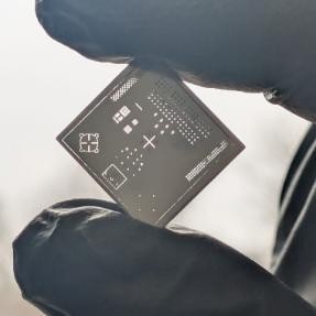
Smart Metal Core. Courtesy of Lux Semiconductors.
CEG Initiatives
CEG has a long history of supporting the Capital Region’s semiconductor industry, from marketing the region and hosting events at SEMICON West to sponsoring several apprenticeship programs for GlobalFoundries and NY Creates to conducting a microelectronics workforce needs assessment for the Northeast Regional Defense Technology Hub (NORDTECH). CEG has also launched a Semiconductor Growth Access Program (SGAP) that aims to broaden the Capital Region’s semiconductor supply chain by providing targeted businesses with funding for legal, financial, business planning, and technical accounting assistance.
Don’t miss these insights into the trends that are shaping the Capital Region’s economy. Sign up for CEG’s e-news and follow us on:
![]()
![]()
![]()